Journal of Physical Chemistry & Biophysics
Open Access
ISSN: 2161-0398
ISSN: 2161-0398
Conference Proceeding - (2015) Volume 5, Issue 6
InAs/GaSb superlattice (SL) is a promising material system for high performance infrared detector. The electrical and optical properties are directly governed by the composition and the periodicity of the InAs/GaSb cell. In particular, several structures with different InAs to GaSb thickness ratios in each SL period, can target the same cut-off wavelength and exhibit different type of conductivity, n-type or p-type. Consequently, by using specific SL periods, it is possible to design a midwave infrared pin photodiode without intentionally doped the structure. Electrical and electro-optical characterizations, of such device fabricated by molecular beam epitaxy, are reported.
<Keywords: InAs/GaSb superlattice; Infrared detector; Photodiode
The use of InAs/GaSb superlattice (SL) material as absorbing zone of IR photodetector was first proposed by Smith and Mailhot [1] in the end of the 80's. Their original proposition was motivated by favorable theoretical optical and electrical properties combined with the possibility to address a wide range of infrared wavelength. Indeed, due to an unusual type-II broken gap alignment, the InAs/GaSb SL quantum structure allows midwave infrared (MWIR) and longwave infrared (LWIR) absorption while being lattice-matched to the GaSb substrate.
The first SL pin photodiodes, operating in the MWIR and in the LWIR, were fabricated in the 90's [2,3] and twenty years later, the progresses, both on the epitaxy and processing of this material, have been so extensive [4] that SL technology is now commercially available for advanced MWIR imaging applications [5].
Among SL properties, one of the main interests is that several structures, with different InAs to GaSb thickness ratios in each SL period, can target the same cut-off wavelength. Recent work reported photodiodes with different SL periods having the same cut-off wavelength at 5 μm at 77K [6]. This study shows the influence of the SL composition on dark current measurements and shape of spectral responses.
The type of conductivity of the nid region is also linked to the InAs/ GaSb SL period. Indeed, because the nid GaSb and InAs layers have p-type and n-type residual backgrounds, respectively, the background of the nid SL active region is likely to be either n-type or p-type. The InAs/GaSb SL tends to result in n-type material for thicker InAs layer ("InAs-rich" structure) whereas thicker GaSb layer ("GaSb-rich" structure) makes the material p-type [7].
The objective of this paper is to report results on SL pin photodiodes operating in the MWIR spectral domain at 77K and to use the flexibility properties of SL quantum structure, in cut-off wavelength and doping, to design and then to fabricate by Molecular Beam Epitaxy (MBE), a pin photodiode where the active zone is made of different SL periods (Figure 1).

Figure 1: Schematic view of the pixel pin photodiode where the active zone is made of different SL period composition for MWIR operation.
The InAs/GaSb heterointerface presents an indirect broken gap type-II band alignment where the conduction band of the InAs layer is lower than the valence band of the GaSb layer. In this configuration, the electrons are mainly located in the InAs layers, whereas holes are confined in the GaSb layers. Consequently, the band gap of the SL, determined by the energy difference between the first electron miniband C1 and the first heavy hole state V1, depends only on the layer thicknesses, in symmetric (same thickness of InAs and GaSb layers) or asymmetric (one of the two layer thicker than the other) configurations. To quantify the symmetric or asymmetric period design, we define the quantity R as the InAs to GaSb thickness ratio in each InAs/GaSb SL period: R=InAs/GaSb. R=1 corresponds to symmetric structure, R>1 suits to "InAs-rich" structure while R
A modified envelope function approximation (EFA) model [8], using a short-range delta function potential at each InAs-GaSb interface has been shown to sufficiently predict the band structure of MWIR SLs [9], and is used to calculate SL structure miniband energies. Figure 2 reports the evolution of the calculated fundamental interminiband V1C1 energy transitions at 77K as a function of the SL period thickness, for three different thickness ratio R. This figure highlights the flexibility on cut-off wavelength of the InAs/GaSb SL structure. Indeed, many InAs to GaSb thickness ratios R can target the same cut-off wavelength. The same bandgap around 248 meV (λc=5 μm) at 77K can be obtained by several SL structures. The first structure has a "GaSb-rich" composition with 10 MLs of InAs and 19 MLs of GaSb per period (10/19 structure with R~0.5), the second one is a "symmetric" 10 MLs/10 MLs structure (10/10 structure with R=1), and the last one is a "InAs-rich" configuration where the period is made of 7 MLs InAs /4 MLs GaSb (7/4 structure with R~1.75).

Figure 2: Calculated interminiband SL bandgap at 77K as a function of the SL period thickness (1ML=3Å) for three different thickness ratio R=InAs/GaSb:
These structures were used as absorbing zones (1 μm thick) of pin structure, fabricated by MBE on p-type GaSb substrate. Several structural characterizations were routinely performed on SL samples in order to evaluate the material quality. High material quality of the three samples was confirmed through high-resolution X-ray diffraction measurements (Figure 3). The lattice-mismatch of the SL with the GaSb substrate was less than 50 arcsec and the measured SL period thicknesses are equal to 91.5 Å, 60.7 Å and 32.9 Å for the “GaSbrich”, the “symmetric” and the “InAs-rich” samples, respectively, in agreement with the SL period values (Figure 2).

Figure 3: High resolution X-Ray diffraction spectrum of the three structures: GaSb-Rich, symmetric and InAs-Rich.
To confirm the targeted bandgap, photoluminescence (PL) measurements were performed on the three SL samples. Figure 4 displays the normalized PL spectra of the three structures at 77K, showing PL peaks very close to the value of 5 μm. However, for these three SL structures, we can easily observe that shape and full width at half maximum (FWHM) of the PL spectra are very different. This result indicates that the same bandgap can have dissimilar SL structures.

Figure 4: Normalized PL spectra of SL samples with three different thickness ratio R, showing the same bandgap (λc=5 μm) at 77K.
From epitaxial SL material, circular mesa photodiodes are fabricated using standard photolithography [10] with a mask set containing photodiodes with several diameters, from 60 μm up to 310 μm. Then, the SL devices were placed in a LN2-cooled cryostat in order to perform photoresponse measurements.
Dimensionality behaviour of SL MWIR photodiodes
Figure 5 shows the non-calibrated spectral response of the three photodiodes measured at 77K in similar conditions. As expected, the absorption band edges are the same for the three devices, close to 250 meV (λ~5 μm). The shape of the spectra are nonetheless quite different, with a very sharp absorption close to the bandgap energy for the "GaSb-rich" SL sample, whereas the signal gradually changes around this energy for the “InAs-rich” SL sample. The shapes of these photoresponse spectra are the signatures of inter-miniband absorption in the SL structure, directly proportional to the joined density of states. To correlate the spectral lineshapes with absorption, the density of states DCV was calculated using a metric space with a noninteger dimension α [11] (eq. 1). The result is shown in the inset of Figure 5 for 2 ≤ α ≤ 3.
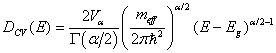

Figure 5: Non-calibrated photoresponse spectra of the three SL photodiodes measured at 77K. In inset, density of states plotted in the framework of the fractional dimensional space (αD space), for dimensionality varying from α=2 to α=3.
where meff stands for electron (mC) or hole (mV) effective masses.
In the case of "GaSb-rich" SL structure, the strong localization of the holes in the GaSb layer induces in a step-like joint density of states, and thus an absorption spectrum comparable to the case of a bidimensional multiquantum-well structure. By contrast, the "InAs-rich" SL structure presents very wide mini-bands for the carriers, especially for the electrons, leading to density of states and then absorption similar to that of a tridimensional bulk material, with a square-root dependence on the energy. The symmetric SL structure is an intermediate situation exhibiting photoresponse spectrum between the 2D and 3D quantumconfined system. Same behavior can be observed on the PL spectra (Figure 4). We also find out that "GaSb-rich" structure tends to show an asymmetric lorentzian shape of a bidimensional structure while the "InAs-rich" structure presents a symmetric gaussian shape of a tridimensional bulk material.
Type of doping of SL MWIR structures
Specific non-intentionally doped (nid), 10/19 "GaSb-rich" and 7/4 "InAs-rich" SL structures were fabricated by MBE on GaSb substrate to performed Hall effect measurements as a function of temperature, using magnetic field B=1T. Particular process, in order to remove conductive GaSb substrate, was made [12]. The sample were front side bonded on host substrate using liquid epoxy adhesive and, after partial mechanical polishing, the substrate was wet etched in a diluted Cr0M3 / HF based solution. Deduced from Hall measurements, temperature dependence of the effective carrier concentration nH and type of doping at 77K for the "GaSb-rich" and "InAs-rich" SL structures, are presented in Figure 6.

Figure 6: "InAs-rich" and "GaSb-rich" SL structures : Measured apparent Hall carrier concentration NH as a function of 1/T (a) ; Hall resistance as a function of magnetic field at 77K, showing n-type (negative slope) and p-type (positive slope) of doping, respectively (b).
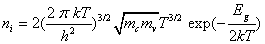
Following type of residual doping of InAs and GaSb compounds, nid "InAs-rich" and "GaSb-rich" SL samples are, respectively, n-type and p-type, at 77K. At low temperature, the samples show carrier concentration equal to 8 × 1014 cm-3 for the n-type "InAs-rich" SL structure and 5 × 1015 cm-3 for the p-type "GaSb-rich" SL sample. At high temperature, it is possible to the extract intrinsic carrier concentration ni given by the equation 2:
 (2)
(2)
ni value about 1 × 1016 cm-3 and 2.5 × 1016 cm-3 at T=300K can be deduced, for the "InAs-rich" and "GaSb-rich" structures, respectively. Thses values are in agreement with recent calculations performed on same SL designs [13].
MWIR SL photodiode using combined properties
Versatile properties on absorption band-edge and doping of "material-rich" SL structure were used to define MWIR pin photodiode. Combining "InAs-rich" and "GaSb-rich" nid SL structures, it is possible to fabricate a pn junction without doping the layers. Because of the steplike 2D absorption (Figure 5) and a higher quantum efficiency at a lower bias voltage than the "InAs-rich" structure [14], "GaSb-rich" structure was used as absorbing layer. The dopant-free SL photodiode, displayed in inset of Figure 7, was grown by MBE on p-type GaSb (100) substrate. The p-type absorbing layer was made of 1.5 μm thick of nid "GaSb-rich" SL while the n-type layer was provided by a 200 nm thick of nid "InAsrich" SL structure. Figure 7 shows the photoresponse spectrum of the processed dopant-free photodiode measured at 80K with a Fourier transform infrared (FTIR) spectrometer. This spectrum reveals a cutoff wavelength at 4.65 μm and clearly exhibits a bidimensional spectral shape which is a signature of "GaSb-rich" SL detector.

Figure 7: Spectral photoresponse of the InAs/GaSb SL photodiode with a dopant-free pn junction at 80K. In inset, schematic diagram of the dopingfree pn junction made by MBE.
Electrical measurements (J-V characteristics) performed in dark conditions at different operating temperatures, ranging from 77K to 225K, were made using a Keithley 6517A electrometer to both apply the bias voltage and read the current delivered by the device. J-V curves are reported in Figure 8. At 77K, dark current density of 3.3 × 10⁻⁸ A/ cm2 at a reverse bias of 50 mV was measured and R0A product value equal to 2 × 10⁶ Ω.cm2 was extracted at 0 V. These values are among the best reported for SL MWIR photodiodes having a cut-off wavelength at 4.65 μm at 77K [15].

Figure 8: InAs/GaSb SL photodiode with a dopant-free pn junction: Dark current density-voltage characteristics for different operating temperature from 77K to 225K.
The InAs/GaSb superlattice is a special quantum system showing non-conventional properties. In particular, same bandgap energy can be addressed by different SL period structures and the residual doping of nid SL structures are directly dependant of the SL period composition. By using these specific properties, a dopant-free pn junction of a InAs/GaSb SL MWIR photodiode was defined and fabricated by MBE. The pn junction was composed by two different non-intentionally doped SL structures with p ("GaSb-rich" structure) or n ("InAs-rich" structure) residual carrier concentration having the same bandgap. Electrical characterizations performed on the SL device confirmed the presence of a diode with results at the state of the art for InAs/GaSb SL photodetector having cut-off wavelength at 4.65 μm at 77K. Such result demonstrates the possibility to fabricate InAs/GaSb SL photodiode without intentional doping the active zone of the pin detector.
This work is supported in part by the French agency "Direction Générale de l'Armement".