Journal of Theoretical & Computational Science
Open Access
ISSN: 2376-130X
ISSN: 2376-130X
Research Article - (2017) Volume 4, Issue 2
The Structural, electronic and chemical bonding of the Sn doped PbX (X=S, Se, Te) are calculated by full potential linearized augmented plane wave method (FP-LAPW) within density functional theory (DFT). Generalized gradient approximation of Wu and Cohen (WC-GGA) is used for calculating the exchange correlation effects. The structural parameters changes with respect to doping. The calculations show that the band gap decreases with the increase of Sn concentration. It has observed that the s, p and d states of PbX (X=S, Se, Te) control their electronic properties. The alloys Pb1–xSnxS, Pb1–xSnxSe and Pb1–xSnxTe show covalent bonding nature which enhances by increasing the Sn concentration.
<Keywords: Density functional theory; Generalized gradient approximation; Density of state; Structural properties; Electronic properties
Computational materials science is an emerging field in condensed matter physics. Computational techniques have come to the level of experiment nowadays. One can determine the physical properties of a material even without the information of experimental data [1,2]. The recent development of computational power allows one to study very complex systems.
In 1874, IV-VI semiconductors were started to be utilized in solid state electronic devices after the Ferdinand Braun’s report on electrical rectification by PbS [3]. After this discovery, PbS also utilized as a rectifier in radios. In recent era, the IV-VI semiconductors have many applications in optoelectronic devices which are mainly utilized for emission and detection of mid-infrared radiations. The IV-VI semiconductors consist of binary compounds PbS, PbSe, and PbTe and their alloys i.e., PbSnSe, PbSnTe, PbSrSe, PbEuTe etc. [4]. They are used in diode lasers [5], long wavelength imaging [6], and in also thermo photovoltaic devices [7]. They are also utilized to control pollution and gas spectroscopy, remote sensing, thermograph, chemical sensing etc. [8,9].
At normal temperature and pressure Lead sulfide (PbS) rock-salt structure is a narrow band gap semiconductor material. Its band gap is direct and equal to 0.45 eV at room temperature [10]. Lead selenide (PbSe) is also a direct band gap semi-conductor material which has a stable rock-salt structure. The band gap of PbSe is equal to 0.16 eV at 4 K [11]. Lead telluride (PbTe) is direct band gap material and its band gap is equal to 0.29 eV. It also exists in rock salt structure at normal temperature and pressure [12]. Tin sulfide (SnS) is a narrow indirect band gap of 1.07 eV and the direct band gap occurs at energy of 1.3 eV [13]. The structure of SnS is orthorhombic but it changes to rock-salt structure at high temperature. Tin selenide (SnSe) is also an orthorhombic crystal and become rock-salt at high temperature as well [14]. Tin chalcogenide (SnTe) is a narrow direct band gap semiconductor with a value of 0.35 eV. It exists in rock-salt (RS) structure at ambient conditions [15].
With doping Sn in PbX (X=S, Se, Te), ternary compounds Pb1– xSnxTe, Pb1–xSnxSe, PbS1–xSex have been experimentally grown at various concentrations [9]. These materials are widely used for optoelectronic applications e.g., photovoltaic sensors. These photovoltaic IV–VI semiconductor infrared sensors (Pb1–xSnxTe, Pb1–xSnxSe, PbS1–xSex, PbTe etc.) are as sensitive as Hg1–xCdxTe, and can fabricate easily especially on Si substrates. However, the technology of photovoltaic lead compound selection is behind that of Hg1–xCdxTe alloy [9].
Computational techniques have many advantages in material science due to no restrictions in these techniques. We can easily model all types of materials by computational techniques. The ab-initio or first principle study is the approach to finding the various properties of a material by just knowing its structure and composition [16]. This technique has an advantage over real experiment because we have all controls over all variables in material for stimulations. This control helps us to design a practicable experiment for understanding the material’s behavior on a specific variable. From this calculation, it is very easy to change the crystal structure, remove or substitute an atom, varying pressure and other changes which will alter on the properties of the material.
Density functional theory (DFT) [17] is usually used to investigate the electronic and structure properties of materials, it can also predict chemical, optical and magnetic properties of the materials i.e., metals, semi-metals, semiconductors and insulators. The density functional theory (DFT) was proposed by Hohenberg and Kohn to simplify the problem and got the noble price in chemistry in 1998. The density functional theory (DFT) is one of the important tools in computational material science for investigation of properties of material such as optical, structural, electronic and magnetic.
This project is completed by performing the calculations through WIEN2K code. This software is based on DFT. FP-LAPW model is utilized in the Wien2k code [18], with different XC- potential. The main two parts are consisting in the Wien2k code. The first is the initialization and the second is the self consistent-field cycle (SCF). Then in every part there are still many programs which will be done step by step to complete these cycles and can be able to find the structural, electronic and Chemical properties of Pb1–xSnxS, Pb1–xSnxSe and Pb1– xSnxTe compounds at concentrations x=0, 0.25, 0.5, 0.75, 1.
Structural properties
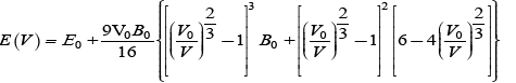
The calculated structural properties of the studied materials are lattice constant a (Aº), Bulk modulus B (Gpa), derivative of bulk modulus B’, unit cell energy E0. Before the discussion of structural properties of ternary compounds Pb1–xSnxS, Pb1–xSnxSe and Pb1–xSnxTe at concentrations x=0, 0.25, 0.5, 0.75,1, we first start the structural properties of binary compounds PbS, PbSe, PbTe, SnS, SnSe and SnTe in rock-salt phase. The Birch-Murnaghan’s equation [19] is used to minimize the total energy with respect to unit cell volume which is given as:
 (1)
(1)
The structure of all binary compounds PbS, PbSe, PbTe, SnS, SnSe, SnTe and ternary compounds Pb1–xSnxS, Pb1–xSnxSe and Pb1–xSnxTe are in sodium chloride (rock-salt) structure. The sodium chloride structure represented a face centered cubic lattice. The structure of binary compounds and ternary compounds are shown in Figure 1. Plots of total energy as a function of volume of Pb1–xSnxS, Pb1–xSnxSe and Pb1– xSnxTe at different concentration of Sn gives unit cell volume Vo, lattice constant a (Aº), Bulk modulus B (Gpa), derivative of bulk modulus B’ and unit cell energy E0 as shown in Figure 2. So the lattice constant and bulk modulus values are in good agreement with experimental values as shown in Tables 1 and 2 and from the tables lattice constant is decreasing as we adding the concentration of Tin (Sn) in PbX (X=S, Se, Te). The maximum lattice constant is at zero doping in the PbX (X=S, Se, Te) and minimum at the doping concentration of x=1. In Pb1-xSnxS the bulk modulus is maximum when Sn is doped at the concentration of x=1 and minimum when the Tin (Sn) is doped at concentration of x=0.
| a(Aº) | B(GPa) | B´ | E0(Ry.) | |
|---|---|---|---|---|
| PbS | ||||
| This work | 5.8893 | 60.7348 | 7.13 | -42652.61 |
| Other works | 6.012d | 52.1d | 4.10e | - |
| Experiment | 5.95a | 52.9d | - | - |
| Pb0.75Sn0.25S This work Other works Experiment |
5.8717 | 62.26 | 5.0 | -141112.67 |
| Pb0.50Sn0.50S This work Other works Experiment |
5.835 | 60.08 | 5.0 | -111614.78 |
| Pb0.25Sn0.75S This work Other works Experiment |
5.796 | 62.01 | 4.12 | -82116.89 |
| SnS This work Other works Experiment |
5.7492 5.848c 5.69b |
64361 | 4.034 | -13154.73 |
aRef [20], bRef [21], cRef [22], dRef [23], eRef [24].
Table 1: Calculated structural parameters of Sn doped PbX(X=S) at variation of Sn concentration along with experimental and other calculations.
| a(Aº) | B(GPa) | B´ | E0(Ry.) | |
|---|---|---|---|---|
| PbSe | ||||
| This work | 6.095 | 56.6262 | 4.5911 | -46714.19 |
| Other works | 6.222a | 47.5a, 49.1a | 4.35c | - |
| Experiment | 6.117a | 54.1a | - | - |
| Pb0.75Sn0.25Se This work Other works Experiment |
6.081 | 52.5234 | 4.4792 | -157359.025 |
| Pb0.50Sn0.50Se This work Other works Experiment |
6.035 | 55.94 | 4.12 | -127861.13 |
| Pb0.25Sn0.75Se This work Other works Experiment |
5.997 | 56.2424 | 4.4051 | -98362438 |
| SnSe This work Others works Experiment |
5.954 6.062b 5.90d |
60798 | 5.0 | -17216.3178 |
aRef [23], bRef [22], cRef [24], dRef [25].
Table 2: Calculated structural parameters of Sn doped PbX(X=Se) at variation of Sn concentration along with experimental and other calculations.

Figure 1: Structure of (a) PbS (b) PbSe (c) PbTe (d) SnS (e) SnSe (f) SnTe (g) Pb0.75Sn0.25S (h) Pb0.75Sn0.25Se (i) Pb0.75 Sn0.25Te (j) Pb0.50Sn0.50Se (k) Pb0.50Sn0.50Se (l) Pb0.50Sn0.50Te (m) Pb0.25Sn0.75S (n) Pb0.25Sn0.75Se (o) Pb0.25Sn0.75Te.

Figure 2: Total energy as a function of volume of (a) PbS (b) PbSe (c) PbTe (d) SnS (e) SnSe (f) SnTe (g) Pb0.75Sn0.25S (h) Pb0.50Sn0.50S (o) Pb0.25Sn0.75Te (i) Pb0.25Sn0.75S (j) Pb0.75Sn0.25Se (k) Pb0.50Sn0.50Se (l) Pb0.25Sn0.75Se (m) Pb0.75Sn0.25Te (n) Pb0.50Sn0.50Te.
Also the energy of Pb1-xSnxS is maximum at concentration of x=0.25 and minimum at the doping concentration of Tin (Sn) at x=1 as shown in Table 1. In Pb1-xSnxSe the bulk modulus is maximum at doping concentration of x=1 and minimum at the doping concentration of x=0.25. Also the energy of Pb1-xSnxSe is maximum at concentration of x=0.25 and minimum at concentration of x=1 as shown in Table 2. In Pb1-xSnxTe the bulk modulus is maximum at concentration of x=1 and minimum at doping concentration of Tin (Sn) at x=0.25 as shown in Table 3. The energy of Pb1-xSnxTe is maximum at concentration of x=0.25 and minimum at concentration of x=1. The bulk modulus and energy of Pb1-xSnxSe and Pb1-xSnxTe are changing in same way as in both samples the bulk modulus is maximum at concentration of x=1 and minimum at concentration of x=0.25, also in the energy case in both samples it is maximum at concentration of x=0.25 and minimum at concentration of x=1 but the parameters i.e., bulk modulus and energy of Pb1-xSnxS is changing in different concentration then Pb1-xSnxSe and Pb1-xSnxTe. In the Figure 3, it shows that lattice constant varies with respect to doping concentration of Tin (Sn).
| a(Aº) | B(GPa) | B´ | E0(Ry.) | |
|---|---|---|---|---|
| PbTe | ||||
| This work | 6.43 | 44.44 | 5.0 | -55446.977 |
| Other works | 6.55c | 39.95c | 4.32c | - |
| Experiment | 6.47a | 39.8c | - | - |
| Pb0.75Sn0.25Te This work Other works Experiment |
6.409 | 46.1301 | 4.4436 | -192290.1989 |
| Pb0.50Sn0.50Te This work Other works Experiment |
6.373 | 46.29 | 5.00 | -162792.31 |
| Pb0.25Sn0.75Te This work Other works Experiment |
6.33 | 47.1526 | 4.6470 | -133294.4232 |
| SnTe This work Others works Experiment |
6.28 6.312b 6.327d |
50.0925 | 4.9679 | -25949.032 |
aRef [26], bRef [22], cRef [24], dRef [27].
Table 3: Calculated structural parameters of Sn doped PbX(X=Te) at variation of Sn concentration along with experimental and other calculations.

Figure 3: Lattice parameter vs. Sn% concentration in PbX (X=S, Se, Te).
Electronic properties
Band structure: The band structure gives useful information about the structure of materials. The band structure of Sn doped PbX (X=S, Se, Te) compounds at different concentration are calculated and shown in Figures 4a-4o respectively. For PbS the band structure is shown in Figure 4a which is in rock salt phase, from figure the minimum of conduction band (CB) and the maximum of valance band (VB) are at L-symmetry point so PbS has a direct band of 0.28 eV. Similarly of PbSe and PbTe have same L-symmetry point and have direct band gaps of 0.48 eV and 0.8 eV as shown in Figures 4b and 4c. From Figures 4d-4f it is clear that SnS, SnSe and SnTe have narrow direct band gap values 0.09 eV, 0.1 eV and 0.07 eV respectively. The compounds Pb0.75Sn0.25S, Pb0.75Sn0.25Se are zero band gap material as shown in Figure 4g and 4j. The Pb0.75Sn0.25Te has a narrow direct band gap 0.082 eV as shown in Figure 4m. In Pb0.50 Sn0.50S Pb0.25Sn0.75S, Pb0.50Sn0.50Se, Pb0.25Sn0.75Se, Pb0.50Sn0.50Te and Pb0.25Sn0.75Te compounds have zero bands gap as shown in Figure 4g, 4h, 4k, 4l, 4n and 4o. So the semiconductor materials become metallic at doping concentration of x= 0.25, 0.50, 0.75 but at doping concentration of x=1 then again there is again narrow band gap. All the band gap values for different compounds at different doping concentration are mentioned in the Table 4. As the band gap occurs in the range of 0-0.8 eV, the fundamental edge occurs in the infrared region. The result matches with experimental one because it’s also show metallic nature at different doping concentrations as mentioned in Table 4 As there are less materials on the band gap of Sn doped PbX(X=S, Se, Te) with which we compare it with our results but we are confident about our results due to use of Wu-Cohen GGA at high k-point value of 5000.
| This work(GGA) | Experimental | Other Calculations | |
|---|---|---|---|
| PbS | |||
| Eg | 0.28 | 0.42c,0.286d | 0.448 d,0.380d |
| Pb0.50Sn0.50S | |||
| Eg | 0 | - | |
| SnS | |||
| Eg | 0.09 | - | - |
| PbSe | |||
| Eg | 0.48 | 0.278b | 0.318 d,0.340 d |
| Pb0.50Sn0.50Se | |||
| Eg | 0 | x=0..~0.2,0.18–0 eV (T=77k)g |
|
| SnSe | |||
| Eg | 0.1 | ||
| PbTe | |||
| Eg | 0.8 | 0.33c,0.19 e | 0.649e |
| Pb0.75Sn0.25Te | |||
| Eg | 0.082 | x=0…~0.4,0.22–0eV (T=77k)g | |
| Pb0.50Sn0.50Te | |||
| Eg | 0 | x=0…~0.4,0.22–0eV (T=77k)g | |
| SnTe | |||
| Eg | 0.07 | 0.35a | 0.19f (300k) |
Pb0.75Sn0.25S, Pb0.75Sn0.25Se, Pb0.25Sn0.75S, Pb0.25Sn0.75Se, Pb0.25Sn0.75Te are zero band gap due to our result. aRef [28], bRef [29], cRef [30], dRef [23], eRef [31], fRef [32], gRef [33]
Table 4: Energy band gaps (in eV) for Sn doped PbX (X=S, Se, Te) compounds at (0 ≤ X ≤ 1) in the rock salt phase along with the experimental and other calculations.

Figure 4: Band structure of (a) PbS (b) PbSe (c) PbTe (d) SnS (e) SnSe (f) SnTe (g) Sn0.25Pb0.75S (h) Sn0.50Pb0.50S (i) Sn0.75Pb0.25S (j) Sn0.25Pb0.75Se (k) Sn0.50Pb0.50Se (l) Sn0.75Pb0.25Se (m) Sn0.25Pb0.75Te (n) Sn0.50Pb0.50Te (o) Sn0.75Pb0.25Te.
Density of states: Density of states (DOS) describes the number of states of a system per unit interval of energy which are occupied by the electrons. Study of band structure, dielectric function, bond character and reflectivity require the knowledge of electron density of states. The DOS of PbS, PbSe, PbTe, SnS, SnSe, SnTe and ternary compounds of Sn0.50Pb0.50S, Sn0.50Pb0.50Se and Sn0.50Pb0.50Te by using GGA scheme are shown in Figures 1 and 5-12. There are four regions in the fundamental density of states. The lower region of VB, the upper region of VB, the lower region of CB and the upper region of CB. DOS of PbS in rock salt are shown in Figure 5. The lower part of VB is started around -8.75 eV and the major contribution at this part is Pb-s state, also a little contribution by the states of S-s and s-p. Now the upper part of VB start about -5.8 eV. The VB near Fermi level is dominated by S-p and also a little contribution by the states of Pb-s and Pb-p. Now the third region is the CB in which the lower part dominated by Pb-p and S-p states and the upper part is due to S-d state.

Figure 5: DOS of PbS.

Figure 6: DOS of PbSe.

Figure 7: DOS of PbTe.

Figure 8: DOS of SnS.

Figure 9: DOS of SnSe.

Figure 10: DOS of SnTe.

Figure 11: DOS of Sn0.50Pb0.50S.

Figure 12: DOS of Sn0.50Pb0.50Se.
For PbSe the lower part of VB is dominated by Pb-s state and also a little contribution of Se-p state. Then after the lower part is the upper part of VB which is near to the Fermi level and has a major contribution due to Se-p state and also a little contribution due to Pb-s, Pb-p, and Pb-d states. Then near to the Fermi level is the CB whose lower part is dominated by the Pb-p and Se-p states. For the upper part of CB the major contribution is due to Se-d state and also little contribution of Pb-s, Pb-p and Pb-d as shown in Figure 6.
DOS for PbTe is the lower part of CB, dominated by Te-s state and also little contribution due to Pb-s state is shown in Figure 7. The upper part of VB is dominated due to Te-p state and also little contribution of Pb-s, Pb-p, Pb-d states. Then in CB the lower part is dominated due to Pb-p and Te-p states and the small contribution is due to Pb-s, Pb-d and Te-d states. The upper level of CB is mainly contributed due to Pb-p and Te-d states.
From figure of SnS it is clear that the lower part of VB is dominated due to Sn-s state and small contribution of Sn-p, S-s and S-p states. Then the upper part is dominated due to Sn-s and S-s states and also small contribution is Sn-p state. The lower part of CB is dominated due to Sn-p and S-p states near the Fermi level and the upper part is dominated due to Sn-p, Sn-d and S-d states and also small contribution of Sn-S, Sn-f and S-p states as shown in Figure 8.
DOS of SnSe is shown in Figure 9. The lower part of VB is dominated by Sn-S state and also small contribution of Se-s, Se-p states. Then the upper part has a major contribution of Sn-s and Se-p states and also small contribution of Sn-p and Sn-d states. Then the lower part of CB near the Fermi level is dominated by Sn-p and Se-p states and the upper part is dominated due to Sn-p and Se-d states and also small contribution of Sn-s, Sn-d, Sn-f, Se-s and Se-p states.
It is clear from Figure 10 that the lower part of VB is dominated by Te-s state and also small contribution of Sn-s and Sn-p states. The upper part of VB is due to Sn-s and Te-p states. After Fermi level is the lower part of CB which is dominated by Sn-p and Te-p states and for the upper part it is dominated by Sn-d and Te-d states.
For the compound Sn0.50Pb0.50S the DOS is shown in Figure 11. The lower part of the VB is dominated due to Sn-s and Pb-s states and also small contribution of S-s and S-p states. Then the upper part of VB is dominated due to S-p state and also a small contribution of Sn-s, Pb-s, Sn-p, Pb-p and Pb-d states. Then for lower part of CB which is near to Fermi level is dominated by Sn-p, Pb-p and S-p states and also small contribution of Sn-s, Sn-d, Pb-d and S-d states. For upper part of CB is dominated by S-d state.
The DOS of Sn0.50Pb0.50Se is shown in Figure 12. In figure the lower part of VB is dominated by Sn-s and Pb-s states and also small contribution of Se-s and Se-p states. Then after the lower part there is upper part of VB which has a major contribution of Se-p state and also small contribution of Sn-s, Sn-p, Pb-s and Pb-p states. The lower part of CB is dominated by Sn-p state and the upper part is dominated by Se-d state.
The lower Te-s state band is dominated and the small contribution of Sn-s and Pb-s states is shown in Figure 13. Then near Fermi level is the upper part of VB which is dominated by Pb-s and Te-p states and also small contribution of Sn-s, Sn-p and Pb-p states. After the Fermi level is the lower part of CB which is dominated by Sn-p and Pb-p states and also little contribution of Sn-s, Sn-d and Te-d states. The upper part of CB is dominated by Sn-d, Pb-d and Te-d states.

Figure 13: DOS of Sn0.50Pb0.50.
Electron density: The chemical bonding properties can be defined by the charge density distribution in a solid. The nature of bonding can be described by electron density i.e., ionic or covalent bond between the cation and anion. The electron density plots of Sn doped PbX(X=S, Se, Te) at different concentration are shown in Figure 14a-14i. The electron density plots of these compounds are in rock salt phase at (110) plane. It is clear from figures that the electron density plot of compounds is covalent nature. By adding Sn concentration in the compounds PbX(X=S, Se, Te) the nature of covalent bond becomes stronger.

Figure 14a: Electron charge density of PbS at (110) plane.
Figure 14b: Electron charge density of PbSe at (110) plane.

Figure 14c: Electron charge density of PbTe at (110) plane.
Figure 14d: Electron charge density of SnS at (110) plane.

Figure 14e: Electron charge density of SnSe at (110) plane.
Figure 14f: Electron charge density of PbTe at (110) plane.

Figure 14g: Electron charge density of Pb0.75Sn0.25S.
Figure 14h: Electron charge density at (110) plane of Pb0.75Sn0.25Se at (110) plane.

Figure 14i: Electron charge density of Pb0.75Sn0.25Te at (110) plane.
The Structural, electronic and chemical bonding, of the Sn doped PbX (X=S, Se, Te) are calculated by full potential linearized augmented plane wave method (FP-LAPW) within density functional theory (DFT). The Sn doping concentration for Pb1–xSnxS, Pb1–xSnxSe, and Pb1–xSnxTe is in the range x=0 to x=1 in step of 0.25 in the rock salt phase. By doping Sn in PbX(X=S, Se, Te) the lattice constants decreases linearly by increasing the concentration. The electronic properties also changes with respect to the composition of the materials. The band gap plots of PbX (X= S, Se, Te) show the direct band gap (L-L) nature. The direct band gap is found to vary by doping Sn in PbX(X=S, Se, Te). So the direct band gap of the ternary alloys varies in the range 0- 0.8 eV. It has observed that the s, p and d states of PbX (X=S, Se, Te) control their electronic properties. The alloys Pb1–xSnxS, Pb1–xSnxSe and Pb1–xSnxTe show covalent bonding nature which enhances by increasing the Sn concentration. Hence it is concluded from this study that the Sn doing PbX(X=S, Se, Te) varies the physical properties widely and the resulted materials become more suitable to use in Infrared detectors, Braggs reflectors and optical devices working in lower frequency regime.