Journal of Physical Chemistry & Biophysics
Open Access
ISSN: 2161-0398
ISSN: 2161-0398
Research Article - (2023)Volume 13, Issue 1
In this research, we design a plasmonic refractive index sensor and examine it numerically, using transparency, refractive index, sensitivity, FOM fit shape and Q quality factor, to optimize and improve performance quality. We will be to design the structure of this sensor, we use two plasmonic waveguides, a cavity, two rings and two teeth. The resonant wavelengths and refractive index of the resonators are investigated and simulated by the Finite Difference Time Domain (FDTD) method, and we draw the obtained diagrams using MATLAB software. After completing the sensor design, due to the fact that the amplifiers are very sensitive to changes in the refractive index, so by changing the refractive index and changing the dimensions of the structure, we can weaken or strengthen the passage coefficient in the resonant modes. These plasmonic sensors with a simple frame and high optical resolution can be used to measure refractive index in the medical, chemical and food industries.
Photonic; Plasmonic; Surface plasmons; Waveguide; Resonators; Optic
Surface Plasmon Polaritons (SPPs) have been studied extensively recently due to the fact that they confine light at nanoscale dimensions [1]. As a result of these unique features, SPPs are used in many structures such as filters [2], optical demultiplexers, bio-sensors [3-20], logic gates and etc. The Metal-Insulator-Metal (MIM) optical waveguide is used extensively for design of many plasmonic devices due to its ability to confine light within a small area and its compatibility with electronic platforms [21-30]. In addition, having a simple design procedure makes it one of the most favorable structures. Consequently, a diversity of MIM plasmonic devices have been designed and implemented. Some of them are optical filters, sensors, coulpers, slow light devices, splitters and all-optical switches. A good refractive index sensor needs to have a good sensitivity (S) and a high Figure of Merit (FOM). Increasing the device size usually increases the sensitivity, but larger structures have higher full width half maximum, which leads to a reduction of FOM. Many criteria can be used to implement refractive index sensors, but plasmonic sensors are more suitable for integrated circuits due to their very small size (nanometers). Recently, various types of plasmonic sensors have been designed and manufactured. Among them, plasmonic refractive index sensors require high sensitivity and resolution. Conventional plasmonic sensors consist of a MIM waveguide with a cavity. Such cavities can have a variety of geometries such as tooth-shaped, disc-shaped, ring-shaped, and so on. In this paper, we propose a MIM plasmonic sensor with two rings and a cavity and two teeth. To simulate the sensor, the two-dimensional Finite Difference Time Domain (FDTD) method with a uniform mesh size of 8 nm has been used. The boundary condition for all directions is selected as the Perfectly Matched Layer (PML).
Structural model and theory analysis
There are many structures for designing optical sensors. These optical sensors usually include amplifiers and waveguides. Each waveguide with any geometric shape has the ability to transmit waves and can limit their energy in one and two dimensions. The proposed structure is shown in Figure 1, which includes two waveguides and a cavity, and two rings and two teeth. The input wave goes from the left waveguide to the structure and after passing through them goes to the output waveguide. The width of the two waveguides is w1=50 nm. The middle ring is located in the middle of two waveguides that have an inner radius of r1=90 nm and an outer radius of R1=w133 nm, which is located at a distance of 19 nm from the two waveguides. The two teeth are connected to the middle ring, which has a length of 40 nm and a height of 20 nm. A ring is located at the bottom of the right waveguide and has an inner radius of r1=91 nm and an outer radius of R1=126 nm. The cavity also has a length of L=80 nm and a height of W2=200 nm. The lower ring is attached to the waveguide and the cavity and the distance from the cavity to the waveguide is 55 nm. Pin and Pout are the monitors for measuring the input and output waves, respectively, and the transmission is calculated by T=Pout/Pin.

Figure 1: Two-dimensional image of a plasmonic sensor.
As shown in the 2D image, the green and white areas represent silver and air, respectively. The air permittivity is set to ε=1 and the silver permittivity is used using the greeting model as follows:
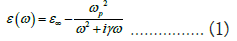
Here c∞ gives the medium constant for the infinite frequency, ωp refers to bulk frequency for plasma, γ means damping frequency for electron oscillation, and ω shows incident light angular frequency. The parameters for silver are c∞=1, ωp=1.37 × 10¹⁶ Hz, and γ=3.21 × 10¹³ Hz. Only TM mode is available in the structure. According to Figure 1, the TM wave, which is used for SPP excited waves, starts propagating from the left waveguide and propagates in the waveguide, and its intensity decreases as it gets closer to the output port. After distributing the field at the resonant frequency of the simulated structure, each amplifier reflects a certain amount of input wave.
Fracture coefficient simulation and measurement methods
The resonant behavior of the proposed structure is examined numerically and theoretically. In the numerical approach, we use the Time Domain Finite Difference (FDTD) simulation method with Perfectly Matched Layer (PML) boundary conditions because this method effectively reduces the numerical reflection. The uniform mesh size is 8 nm. First, to measure the performance of the sensor and increase its quality, we must change its refractive index. This is done in the wavelength range of 400 nm to 1500 nm and the refractive index of the middle ring will change in steps of 0.01 from 1.15 nm to 1.2 nm. An electromagnetic field is generated by the excitation of a sensing element using light generated by SP that is concentrated on the metal surface. The refractive index of the MIM changes when the material under contact contacts the sensor. SPs are very sensitive to changes in refractive index in the vicinity of the surface. The reason we have only changed the refractive index of one ring and the refractive index of other amplifiers remains the same is to achieve a better result and a stronger sensor design. The transmission spectrum from the sensor device is shown in Figure 2.

Figure 2: Transmission spectra of plasmonic refractive index sensor.
After comparing the wavelengths using the refractive index change and plotting the transmission spectrum, we must obtain the three criteria of sensitivity S and the shape of the FOM and the quality factor Q. With this, we create a technology map to define the standard and development process of optical refractive index sensors. Sensitivity S defines the ratio of the output wavelength change of the sensor to the refractive index changes and is obtained from the following relation:
S = Δλ / Δn(nm / RIU) ……………. (2)
We see the diagram of the plasmonic sensitivity coefficient in Figure 3, which according to the figure, has the highest sensitivity for the refractive index n=1.2 (in mode 2) which is equal to 2359 nm/RIU and the lowest value for the refractive index n=1.16 (in mode 1) Which is equal to 314.1 nm/RIU.

Figure 3: Plasmonic sensor sensitivity coefficient diagram.
Resonance wavelength versus refractive index analysis. Note: 
The next item is the Figure of Merit (FOM), which determines the sensitivity of the SRI to the resonance width curve (FWHM) and how accurately the minimum resonance can be measured. FOM is calculated as follows:
FOM = SRI FWHM ……………. (3)
We see the diagram of the Figure of Merit (FOM) in Figure 4, which according to the figure has the highest value for the refractive index n=1.18 (in mode 1) which is equal to 15.03 and the lowest value for the refractive index n=1.12 (in mode 1) which is equal to with 7.354.

Figure 4: Plasmonic sensor FOM diagram. Note: 

And the last case is the quality factor Q, which is obtained from the following equation:
Q = λres /FWHM ……………. (4)
We see the quality factor Q diagram in Figure 5.

Figure 5: Quality factor diagram of Q plasmonic sensor. Note: 
According to the figure, the highest value of quality factor Q is for refractive index n=1.17 (in mode 1) which is equal to 16.56 and the lowest value for refractive index is n=1.19 (in mode 2) which is equal to 7.379. These three factors (S and FOM sensitivity and Q quality factor) and their numerical values showed that this sensor has good performance and quality and has a higher sensitivity compared to similar articles.
In this paper, a very high resolution refractive index optical sensor is presented. It is based on plasmonic conductors of metal-metal insulation. The structure is numerically simulated using the finite difference time domain method. The proposed structure is thought to consist of two plasmonic waveguides, a cavity, two rings and two teeth. This sensor provides a sensitivity of 2359 nm/RIU and a maximum rating of 15.0316 RIU-1 (FOM). Due to its high resolution, this sensor can easily change 0.01% in the analytic refractive index for the index in the range of 1.15-1.2.
[Crossref] [Google Scholar] [PubMed]
[Crossref] [Google Scholar] [PubMed]
[Crossref] [Google Scholar] [PubMed]
[Crossref] [Google Scholar] [PubMed]
[Crossref] [Google Scholar] [PubMed]
[Crossref] [Google Scholar] [PubMed]
[Crossref] [Google Scholar] [PubMed]
[Crossref] [Google Scholar] [PubMed]
[Crossref] [Google Scholar] [PubMed]
[Crossref] [Google Scholar] [PubMed]
[Crossref] [Google Scholar] [PubMed]
[Crossref] [Google Scholar] [PubMed]
[Crossref] [Google Scholar] [PubMed]
[Crossref] [Google Scholar] [PubMed]
[Crossref] [Google Scholar] [PubMed]
Citation: Abbasi H (2023) Plasmon-Induced Flexibility and Refractive Index Measurement in a Sensor Designed by a Cavity, Two Rings, Two Teeth and Two Plasmonic Waveguides. J Phys Chem Biophys. 13:339.
Received: 10-Jun-2022, Manuscript No. JPCB-22-17879; Editor assigned: 13-Jun-2022, Pre QC No. JPCB-22-17879 (PQ); Reviewed: 27-Jun-2022, QC No. JPCB-22-17879; Revised: 26-Dec-2022, Manuscript No. JPCB-22-17879 (R); Published: 02-Jan-2023 , DOI: 10.35248/2161-0398.23.13.339
Copyright: © 2023 Abbasi H. This is an open-access article distributed under the terms of the Creative Commons Attribution License, which permits unrestricted use, distribution, and reproduction in any medium, provided the original author and source are credited.