Journal of Aeronautics & Aerospace Engineering
Open Access
ISSN: 2168-9792
ISSN: 2168-9792
Review Article - (2023)Volume 12, Issue 1
Technical analysis of the performance optimization of nanospintronics devices and quantum computing with electron/nuclear spins has been presented in this paper. Mathematical formulation and a brief theory of these concepts have been briefly discussed. A qualitative review of some of important nanospintronics based devices and Applications of Laser Microscopy to Aerospace Industry, has also been given in the present paper. The paper should be useful to the designers and engineers in the field of nanospintronics devices.
Nanospintronics devices; Quantum computing with electron/nuclear spins; Laser microscopy; Aerospace
In nanospintronics, the focus is on basic research in the three areas of metal semiconductor and molecular/atomic based spintronics with the visionary goal of developing nanoscale spintronic devices based on a detailed knowledge of the underlying atomistic spin-dependent interactions and processes (Figure 1).
Spintronics makes use of the electron's spin degree of freedom to realise electronic devices and functionalities not achievable by only the electron's charge degree of freedom. Recent research activities are focused on novel spin effects in magnetic, nonmagnetic and nanostructures. The main experimental tool is a cryostat with a vector field magnet and microwave frequency electrical access. Direction of effective magnetic field due spinorbit interaction observed in GaMnAs, as shown below:

Figure 1: Direction of the effective magnetic field due spin-orbit interaction in GaMnAs.
In exploring the concepts and applications of spintronics, researhers are interested in studying the role of the spin-orbit interaction in ferromagnetic devices, and have been recently focusing on spin-orbit effects in ferromagnetic semiconductors. It has been understood that the spin-orbit interaction couples the momentum of the charge carriers, and therefore the electrical current, to the carrier spin. Therefore, by passing a microwave frequency current through a device, an oscillatory spin polarization is induced, which causes through the exchange interaction, a torque to act on the magnetic moments. Hence, it is possible to excite resonant precession of the magnetic moments, providing a way to study the spin-orbit interaction and the dynamic properties of nano scale ferromagnets.
It is now understood that as spintronics is entering the phase of nano, new phenomena are coming into observation as a result of interplay between spin dependent transport and electron physics. Seneor, et al. [1] have given a detailed description of the experiments and theories on the interplay between Coulomb blockades and spin properties in structures in which a single nano object is connected to ferromagnetic leads. Kervalishvilia and Lagutinb [2] have described in great detail the important breakthroughs in the important and evolving subject of semiconductor nanomaterials, which represents an upcoming area of research in the device fabrication by using materials with the spin-polarized transport of the charge carriers. More recently, as discussed by Chopra, many new efforts have been made on the theoretical and experimental investigations on spintronic devices [3-6]. The topic of Nanospintronics focuses on studying novel spintronic effects in small, magnetic as well as non-magnetic semiconductor nanostructures. Spin-orbit driven Ferromagnetic Resonance (FMR) has been established as the technique for characterizing ferromagnets, and evaluating the internal magnetic fields, and the damping. Fang, et al. have demonstrated a new way to excite FMR using internal fields generated by the spin-orbit interaction [7].
Nanospintronics and mathematical modeling
In Nanospintronics for magnetic semiconductor material like GaMnAs, when a current passes through such a material, a polarization of the carriers takes place due to the the spin-orbit interaction, because the magnetic moments experience a torque as a result of the exchange coupling between the moments and the carriers. Then the excitation of the resonant precession takes place by the oscillations of the current at the resonant frequency of the magnetic moments, and the detection of the signal by a rectification process produced by the magneto-resistance. Subsequently, the resulting rectification voltage is studied for determining the anisotropy, the intrinsic and extrinsic damping, and the magnitude and direction of the effective fields in the material. The mathematical formulations for the performance analysis and optimization for some of the important nanospintronic devices are technically discussed below.
The double magnetic tunnel junctions are calculated and optimized by evaluating the temperature dependence of the conductance G [8], and the description of the temperature dependence of G on the presence of Kondo effect. The theoretical and experimental investigations have revealed that the temperature dependent part of the conductance is: G~T(-2) for T<<Tk i.e. fermi liquid behavior, and G~(-InT) when T>Tk;
Tk being the temperature corresponding to the Kondo effect. In case of the intermediate temperatures, it is given by:
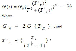
S being the parameter depending on the spin of the impurity in the Kondo effect. The temperature dependence of the conductance G, is evaluated, both for the normal case and also in the presence of Kondo effect. The designer has to consider these factors, and choose them according to the application of the device, and the temperature range of its application.
In case of spin injection, the magnitude (P) of the ensemble spin polarization decreases with time (τ) as well as with distance (d) measured from the injection point (In this case, d is the distance between the injector and the detector). It is found that the decay follows an exponential form, and therefore, the spin relaxation/ diffusion length (or spin relaxation/diffusion time) is conveniently defined as the distance (duration) over which the spin polarization reduces to (1/e) times its initial value. It is thus clear that the case with L>>Ls or τ<<τs, implies complete loss of spin polarization, which means that the spin relaxation phenomenon in the paramagnet tends to bring the nonequilibrium spin polarization back to the equilibrium polarized condition. As we know that the spintronics exploits the non-zero spin polarization, the nanospintronic device designer has to optimize these parameters in order to maximize the efficiency of the device for important applications in Industry, and especially for carrying out research in the premier areas of the field, and the establishments[9,10].
For spin injection from a ferromagnetic to a paramagnet via an interfacial barrier, the spin injection efficiency (η) can be expressed as a weighted average of the conductivity polarizations of the bulk ferromagnetic (PσF), the interface (Pσi) and the bulk paramagnet (PσN). The last quantity (PσN) is zero by definition and the weights are proportional to the corresponding resistances. The spin injection efficiency (η) is given (9) by: Where
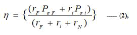
Where rF, ri, and rN represent the effective resistance of the bulk performance optimization of nano spintronics devices and applications of quantum computing and laser microscopy for the spin of the electron is an intrinsic property that is different from the angular momentum due to its orbital motion. Interestingly in a solid, the spins of many electrons can act together to affect the magnetic and electronic properties of a material.
In many materials, it is observed that the electron spins are equally present in both the up and the down state, and no transport properties are dependent on spinthIt can be clearly visualized the a spintronic device requires generation or manipulation of a spin-polarized population of electrons, resulting in an excess of spin up or spin down electron. Thus, a net spin polarization can be achieved by creating an equilibrium energy split between spin up and spin down. This is done by: putting a material in a large magnetic field, exchanging energy present in a ferro magnet or forcing the system out of equilibrium.
Theory of quantum computing with spins based on qubits: In quantum computing, logical operations on individual spins are performed using externally applied electric fields, and spin measurements are made using currents of spin-polarized electrons. Interestingly, the realization of such a computer is dependent on future refinements of conventional silicon electronics. The quantum computing is done by using some architecture for Semiconductor implementations. The pioneering work done on this topic is quite important and relevant still at present. These commonly used architectures are given below (Figure 2).

Figure 2: GaAs quantum dots architecture (left).
Quantum computing with electron/nuclear spins is done by using an ideal quit given by:
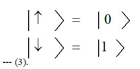
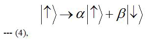
In this ideal qubit, the spin in the upward direction is taken as zero, and that in the downward direction is taken as unity. It is to be understood that in quantum computing, and specifically the quantum circuit model of computation, a quantum gate (or quantum logic gate) is a basic quantum circuit operating on a small number of qubits, which are the building blocks of quantum circuits. However, unlike many classical logic gates, quantum logic gates are reversible (Figure 3). The interaction is studied terms of two types of gates represented by:
1-qubit gate, which functions for Spin rotation, and is given by:
And 2-qubit gate, which functions for Exchange interaction, and is given by:
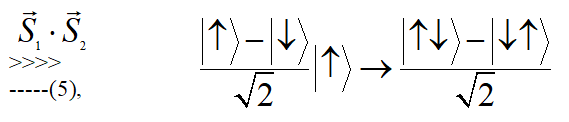
Where, S1.S2 is the spin interaction, in the form of an exchange interaction between 1st and 2nd sites (Figure 3).
Finally, quantum algorithms for doing the functions of Factoring and searching are represented by:
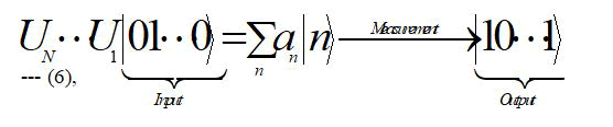
Where U is the controlled U-gate, represented as:

Figure 3: Block diagram for the Simulation of the factoring and searching by quantum algorithms.
It can be understood that the input in the form of the first term on the LHS of this Eqn. is equal to the middle term, which on measurement gives the output in the form of the term on the LHS of this Eqn. Also, |u> is an eigen state of U, |1> being the component in the first qubit.
Today's electronics uses electron charge as a state variable for logic and computing operation, which is often represented as voltage or current. In this representation of state variable, carriers in electronic devices behave independently even to a few and single electron cases. As the scaling continues to reduce the physical feature size and to increase the functional throughput, two most outstanding limitations and major challenges, among others, are power dissipation and variability as identified by ITRS. This paper presents the expose, in those collective phenomena, e.g., spintronics using appropriate order parameters of magnetic moment as a state variable may be considered favorably for a new room-temperature information processing paradigm. A comparison between electronics and spintronics in terms of variability, quantum and thermal fluctuations will be presented. It shows that the benefits of the scalability to smaller sizes in the case of spintronics (nanomagnetics) include a much reduced variability problem as compared with today's electronics. In addition, another advantage of using nanomagnets is the possibility of constructing nonvolatile logics, which allow for immense power savings during system standby. However, most of devices with magnetic moment usually use current to drive the devices and consequently, power dissipation is a major issue. We will discuss approaches of using electric-field control of ferromagnetism in Dilute Magnetic Semiconductor (DMS) and metallic ferromagnetic materials. With the DMSs, carrier-mediated transition from paramagnetic to ferromagnetic phases make possible to have devices work very much like field effect transistor, plus the non-volatility afforded by ferromagnetism. Then we will describe new possibilities of the use of electric field for metallic materials and devices: Spin wave devices with multiferroics materials. We will also further describe a potential new method of electric field control of metallic ferromagnetism via field effect of the Thomas Fermi surface layer.
Some important novel studies on nanospintronic devices and their applications in aerospace
Important study on the topic has been made by Wang, et al., who has used the ideas of modern electronics about electron charge as a state variable for logic and computing operation in terms of voltage or current carriers in electronic devices behaving independently [11]. They have explained the collective phenomenon of spintronics by applying the concept of considering magnetic moment as a state variable in the form of a novel room-temperature information processing system.
Borschel, et al. have studied and discussed the highly Mn-doped GaAs nanowires of high quality crystal structure developed by ion beam implantation [12]. It has been shown that the corresponding magnetoresistance decreases at low temperatures, showing the existence of paramagnetic. It has been emphasized that these findings have the potential for future applications, as a new kind of magnetic material. Pramanik, et al. have given a new concept of the spin transport in organic nanowires to explain for the first time that the spin relaxation time in organics can indeed be very long, and thus making them suitable for research and device making in spintronics, because of the longevity of spin polarization [13]. This is important criterion for nearly all the spintronic devices. Cottet, et al. have discussed various experiments demonstrating gate control of spin transport in a carbon nanotube connected to ferromagnetic leads. Kontos and Cottet have discussed the utility of Nanospintronics for fabricating spin-based quantum bits, in which single spins are able to encode quantum information Nossa and Javier have presented dissertation on theoretical investigations on the electric control of the magnetic properties of molecular magnets. Wickles and Belzig have computed the domain-wall resistance of a Bloch wall situated in a wire of quasi one-dimensional Geometry [14-17]. Lai, et al. have proposed a concept of self-engineered, gate-defined silicon metal-oxidesemiconductor double quantum dot system [18].
Wu has touched upon an entirely new type of usefulness of nanospintronics for data storage, and has derived the dependence of pure spin current signal RS=VS/I measured for two different excitation currents. Koo, et al. has explained the Control of spin precession in a spin-injected field effect transistor [19]. Lee, et al. have presented a review describing in detail the feedback mechanisms, and the progress in selfconsistent simulations and computations of the coupled dynamics, by considering the feedback from the generation of the non-local effective interactions for the magnetization after the summation of the spin accumulation.
Garcia-Raffi, et al. have given a new technique for reducing the sound pressure level in the area of the spacecraft-launcher by placing structures of Sonic Crystals (SCs) at the launch pad for controlling the waves reflecting on it, and have presented their results, which can be very useful in the Aerospace Research and Engineering. It has been well understood that the Robust Optical Materials have applications in Aerospace and Laser Systems. It is important to note that a U.S. Army-funded landmark discovery at New York university is going to change the way researchers develop and use electro-optical devices like lasers, sensors, and photonic circuits over the next decade. The scientists have developed and understood creating of colloids having the unique characteristic of crystallizing into the diamond, a result that is being used in fabricating many components in Aerospace Industry.
It has been reported that the global photonic crystals market outlook for 2019-2024, is that there are going to be a number of jobs for aerospace engineers in qerospace and defense sector. Zhang, et al. have set the aircraft state of Mach 5 as the target operating condition, and have simulated the PC thermal protection ability by the method of computational fluid dynamics. The designers have to confirm some fundamental design aspects of the operation of Spin Engine, and also achieve its reproducibility by controlling at the atomic level, both the position and properties of the PM centers in a suitable solidstate device, for implementing CMOS back-end integration for managing various engineering issues including heat flow and interconnect losses. There are many types of energy generation like from wind, water, and fossil etc. However, Spintronics and Quantum thermodynamics provide a novel approach of the production of ambient power.
Another approach is that of the semi classical model of charge and spin transport based on the drift–diffusion theory, in which we consider transport in metallic/semiconducting no magnets and metallic Ferro magnets, by limiting the diffusion and designing to diffusive dynamics, and assuming that the density and external fields are slowly varying on the scale of the mean free path λ, which is considered to be smaller than the spin diffusion length LSD.
It has to be noted here that spin density implies the excess of total electron density of electrons of one spin over the total electron density of the electrons of the opposite spin. More important is the determination of these four quantities, which have to be computed by using the spin equation. This is a complicated job; and is done by a Spintronics engineer, by solving a set of flux equations; leading to the derivation of these quantities. This is a very complex and tedious job, which requires the skill and expertise of the design engineer, along with long experience of working on such systems. The results are invariably differing slightly from the theoretically collected ones; and so depending on the feedback, the designer has to apply corrections. Generally, three to four iterations are required to achieve the desired results. Sometimes, computer software’s are also used, some of which are even commercially available.
Laser microscopy for testing very tiny components in aeraeronautics and aerospace industry
Laser microscopy is a class of techniques for generating microscopic images, which may be used for testing the tiny components in Aeronautics and Aerospace Industry. In most cases, laser scanning of some sample is done with a diffractionlimited laser beam. Scanning is achieved by moving either the laser beam or the component under test. Light carrying information on the component may be generated in different ways like by scattering, through polarization changes, by second harmonic generation or by exciting fluorescence. The intensity of the light coming from the sample is recorded for each point in it. From these data, images are produced on a computer, and then can be stored in electronic form. In practice, numerical methods are applied to process the images for enhancing the image contrast.
Most commonly used imaging technique is based on a confocal geometry ( → confocal scanning microscopes), where the light from the focus in the component is imaged with a microscopic objective onto a ponhole, behind which the optical power is detected. It can be visualized that this geometry suppresses the influence of light coming from other regions in the component under test, e.g. from before or after the focus, since this light cannot efficiently pass through the pinhole. In fact, mainly the depth resolution is considerably improved. It is interesting to note that for most of the forms of lase microscopy, diffraction limits the possible beam waist radius of the scanning laser beam, and hence the obtained image resolution. However, some techniques allow improving the image beyond the diffraction limit which is called super-resolution microscopy or Nanos copy. Images produced with such microscopes are generally not directly observed through an optical instrument, but in fact are observed on a high-resolution computer screen. The CLSM is a complicated technology with many complicated steps involved, and many different processes are taking place quickly to produce the image on screens. But after learning and getting experience of using the different functions, a number of images and a lot of data can be generated [20].
The field of nanospintronics has been evolving rapidly in the recent years. It is finding useful applications in aerospace, and also in producing ambient energy which in turn is being used for testing the aeronautical devices, since this gives clean energy.
Airbus is exploring a number of quantum technologies that can be applied to aerospace challenges, the most important being quantum computing. It has been realized that the aerospace industry has complex computational needs in the areas of fluid dynamics, finite-element simulations, aerodynamics, and flight mechanics, and actively uses advanced computing solutions in these areas. It is strongly believed that the quantum computing, in tandem with more traditional High Performance Computing (HPC) solutions can help the aerospace industry to solve key huge computational tasks. Many new government agencies and Institutions have been putting lots of funds in developing such materials and energy. It is felt that this evolving field of physics has been finding many novel applications in aerospace industry, and so some very serious attempts should be made to develop this field. For this not only academic institutes, but also big aerospace establishments should make serious research and development efforts to ensure the growth of this field. This has to be emphasized by the scientists working in this area, during their mutual interactions while attending various International Conferences.
[Crossref] [Google Scholar] [PubMed]
[Crossref] [Google Scholar] [PubMed]
[Crossref] [Google Scholar] [PubMed]
[Crossref] [Google Scholar] [PubMed]
[Crossref] [Google Scholar] [PubMed]
[Crossref] [Google Scholar] [PubMed]
Citation: Chopra KN, Walia R (2023) Performance Optimization of Nanospintronics Devices and Applications of Quantum Computing and Laser Microscopy for Instrumentation in Aerospace Industry. J Aeronaut Aerospace Eng. 12:297.
Received: 03-Oct-2022, Manuscript No. JAAE-22-19448; Editor assigned: 05-Oct-2022, Pre QC No. JAAE-22-19448 (PQ); Reviewed: 19-Oct-2022, QC No. JAAE-22-19448; Revised: 17-Jan-2023, Manuscript No. JAAE-22-19448 (R); Published: 24-Jan-2023 , DOI: 10.35248/2168-9792.23.12.297
Copyright: © 2023 Chopra KN, et al. This is an open-access article distributed under the terms of the Creative Commons Attribution License, which permits unrestricted use, distribution, and reproduction in any medium, provided the original author and source are credited.