Advanced Techniques in Biology & Medicine
Open Access
ISSN: 2379-1764
ISSN: 2379-1764
Short Review - (2018) Volume 6, Issue 2
This paper provides an overview of nanocomposite organic electron beam (EB) resist polymers from the viewpoint of advanced techniques for biology and medicine. An outstanding issue with organic devices is the difficulty of simultaneously controlling the lateral size and position of structures at submicron or nanometer scales. Nanocomposite EB organic resist of ZEP520a containing [6,6]-phenyl-C61 butyric acid methyl ester (PCBM) is an excellent electrically conductive material for nanometer lateral-scale organic electronic devices. The distribution of PCBM aggregations in the nanocomposite is examined. The results open the door to the simple fabrication of densely integrated sensitive biosensors with electrical nanowires and single-electron transistors for multiplexed and simultaneous diagnoses.
The detection and quantification of chemical and biological species are crucial to many aspects of healthcare and life sciences, ranging from diagnosis of disease to discovery of new drug molecules. Various devices are now in production or are being developed to meet this need. Radioactive or fluorescent markers are used in many of the devices; however, their use involves time-consuming multi-stage processes that are expensive and unsuitable for real-time detection. Therefore, devices without such markers are desired for detection and quantification.
Field effect transistors (FETs) are sophisticated devices that can be used for label-free and real-time detection of charged molecules in solutions. Detectors based on FETs measure the change in charge accompanying specific molecular recognition events on the gate insulator surface. Biosensors based on Si metal-oxide-semiconductor FETs (MOSFETs) have been developed for detecting various biomolecules, such as, adenosine-5'-triphosphate (ATP) [1], ribosomal protein [2] and target deoxyribonucleic acid (DNA) [3,4]. Recently, FETs composed of nanostructures have attracted attention as a means of detecting target biomolecules in dilute solutions because such nanostructures are very sensitive. For example, biosensors incorporating nanowire FETs are more sensitive than those with wide-channel FETs in a dilute solution of the target biomolecule [5-12]. This is because carriers in a narrow channel are more influenced by a small number of charged biomolecules attached to the gate insulator than those in a wide channel. This is in relation to the fact that the carrier percolation path along the channel easily disappears even with a small number of charged biomolecules in a narrow channel [5]. Using biotin-modified Si nanowire FETs, sensitive detections were achieved for streptavidin (streptavidin and biotin are proteins and ligand-receptor binding of biotin-streptavidin is well known) [6], a single virus of influenza A [7], interactions between ATP and a protein [8] and prostate-specific antigen (PSA) [9,10] (PSA is a protein biomarker for prostate cancer), mouse-immunoglobulin G and mouse-immunoglobulin A [11], target DNA in solution with the probe DNA (12-mer oligonucleotide) attached to the nanowire surface [12]. Another kind of FET having sensitive nanostructures is the single-electron transistor (SET) [13]. SETs have Coulomb islands in the channel and carriers move though the island one by one showing Coulomb oscillations. The high detection sensitivity of SET biosensors for charged biomolecules is due to this Coulomb oscillation. If SETs are to be applied to biosensors, they must be capable of room-temperature operation. Since the charging energy of an electron must be much larger than the thermal energy of room temperature and the charging energy is inversely proportional to the self-capacitance of the island, extremely small nanoscale island structures have to be fabricated as Coulomb islands for room-temperature SET operation. Recently, by making SETs with such nanoscale Si Coulomb island structures for room-temperature operation, biomolecule sensors were demonstrated for the detection of streptavidin [14,15] and PSA [15].
The kinds of FETs used for ion sensors and/or biosensors are not limited to Si MOSFETs. Organic FETs have also been used for labelfree detections of acetylcholine (ACh+) [16], soluble fms-like tyrosine kinase (sFlt1) [17] and DNA [18]. These organic electrical devices have unique advantages of low weight, high mechanical flexibility, cost effectiveness and good chemical structural versatility compared with inorganic devices [19-22]. However, most of the reported devices are over a micrometer in lateral size. An outstanding issue with organic devices is the difficulty of simultaneously controlling the lateral size and position of structures at submicron or nanometer scales. Among the various fabrication techniques, top-down fabrication using electron beam (EB) lithography can form various nanoscale structures with enough positional control for dense integration. However, conventional EB lithography techniques have many problems when they are used for the above purpose. For example, it is difficult to remove only the mask organic resist material by using oxygen plasma ashing or cleaning with a sulfuric acid–hydrogen peroxide mixture because of the small selective etching ratio between the resist and the organic etching object. It is also difficult to obtain a large selective ratio in dry etching between the two. The use of organic devices thus still faces difficulty in regard to simultaneous control of the lateral size and position of carrier conducting structures in the submicron or nanometer region.
For lateral dimensions larger than 5 μm, in contrast, photosensitive electrically conductive organic polymer composites have been reported as materials for which it is not difficult to control the lateral size and position of carrier conducting structures simultaneously. They consist of a photopolymerizable matrix that allows them to be lithographically patterned with photons and have electrical conductivity at the same time. High-aspect ratio structures with a minimum lateral resolution of 5 μm have been fabricated using an electrically conductive photosensitive negative resist of SU8 including silver particles and ultraviolet light [23,24]. A pattern with a line width of about 10 μm was fabricated with electrically conductive SU8 resist materials embedding carbon black particles [25]. These resists are electrically conductive themselves and it is not necessary to use an additional resist for determining the lateral sizes and positions of structures.
Recently, organic EB resist polymers containing fullerenes have been developed as submicron- or nanometer-sized electrically conductive organic materials that allow simultaneous control of the lateral size and position [26]. In these materials, a positive-type EB resist of ZEP520a is used as the matrix organic polymer and fullerenes are incorporated in it (Figure 1). ZEP520a is a copolymer of methyl α-chloroacrylate and α-methylstyrene (Figure 1a). [6,6]-phenyl-C61 butyric acid methyl ester (PCBM) was selected as the fullerene incorporated in the resist (Figure 1b). Before the report, EB resist of ZEP520 into which fullerenes are incorporated had been used only as a mask resist that had improved dry etching resistance for submicron lateral-scale patterning [27- 29]. It had not been used as carrier conducting material of electronic devices and its characteristics related to carrier transport had not been investigated. On the other hand, a number of reports indicated that gate insulating organic polymers containing fullerene molecules, referred to as nanocomposite organic polymers, were promising for organic flash memories because of their relatively simple fabrication techniques [30- 35]. In these nanocomposite organic polymers, the matrix polymers are not EB resist materials. It has been suggested that electrons or holes are injected into and stored in the LUMO or HOMO levels of the fullerenes and the carriers are transferred through the levels in the nanocomposite organic polymers [32,33].
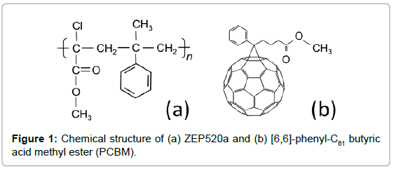
Figure 1: Chemical structure of (a) ZEP520a and (b) [6,6]-phenyl-C61 butyric acid methyl ester (PCBM).
In the above recent report on ZEP520a containing PCBM molecules [26], memory characteristics as well as resist patterning characteristics of the nanocomposite organic EB resist polymer were examined. Figure 2a is a schematic diagram of a capacitor structure fabricated for the capacitance-voltage (C-V) measurements. A ZEP520a layer containing PCBM was formed on a SiO2 layer on an n-type Si substrate. Regarding the memory characteristics, positive flat band voltage shifts ΔVF having substantial magnitudes (|ΔVF|) were observed after applying a negative programming voltage to the capacitors of ZEP520a containing PCBM with excellent retention characteristics, while negligible |ΔVF|’s were observed for those of ZEP520a without PCBM. This suggests that carriers are injected into and transferred through PCBMs in the ZEP520a containing PCBM layer. Moreover, the much larger |ΔVF| after applying the negative programming voltage than after applying the positive programming voltage with the same absolute magnitude (with the same time) for the ZEP520a containing PCBM indicated that electrons were mainly injected into and stored in the LUMO levels of PCBM. These experimental programming characteristics reflect the relative energy difference between the HOMO or LUMO level of PCBM and the Fermi energy EF of the gate Al (Figure 2b). Because the LUMO level of PCBM is closer to the EF of the gate Al than the HOMO level of PCBM is, electrons are preferentially injected into the LUMO levels of PCBM at negative programming voltages, while holes are difficult to inject into the HOMO levels even at positive programming voltages.
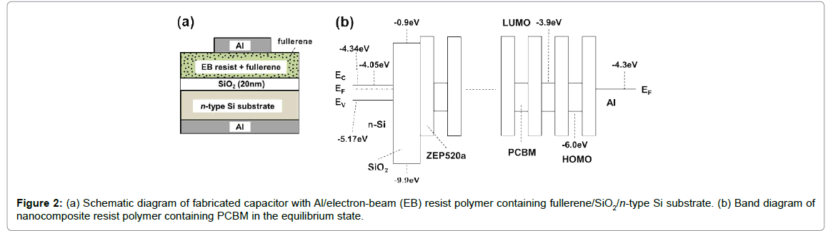
Figure 2: (a) Schematic diagram of fabricated capacitor with Al/electron-beam (EB) resist polymer containing fullerene/SiO2/n-type Si substrate. (b) Band diagram of nanocomposite resist polymer containing PCBM in the equilibrium state.
Regarding the resist patterning characteristics, submicron or nanometer lateral-scale structures have been fabricated simply by EB exposure on ZEP520a containing PCBM and subsequent development. Figure 3 shows a cross-sectional transmission electron microscopy (TEM) image of ZEP520a containing PCBM for a line and space pattern. The designed pitch and line width were 400 nm and 200 nm, respectively. A very clear pattern was formed. The width of the formed line was 140 nm and no resist remained in the space regions on the SiO2 layer where the EB exposures occurred.
There are two white regions, indicated by arrows, near the bottom edges of the resist pattern in Figure 3. These regions are considered to be empty and no resist or PCBM exists. In contrast, there are no white regions in the upper region of the resist pattern. These results suggest that the PCBM molecules aggregated in the bottom region of the line pattern and only the PCBM aggregations in the edge regions of the line dissolved in the developer (ZED-N50) or isopropyl alcohol (IPA) used for rinsing during the development, because part of the aggregation in the edge regions directly contacted the ZED-N50 or IPA. The base diameters of the semispherical PCBM aggregation are about 60 nm and the base center-to-center distance between adjacent aggregations is about 80 nm. Dispersed PCBMs in the upper region are considered to be in a molecular state or in much smaller aggregations than those of the bottom region. Judging from the base diameter and center-to-center distances of these large bottom PCBM aggregations, the minimum side length of a memory cell or the minimum width of a conducting line would be about 200 nm. Optimization of the kind and concentration of incorporated fullerene as well as of the baking conditions of ZEP520a containing PCBM will make it possible to reduce the size of the PCBM aggregation for a further reduction in lateral device size. This will enable the size of the Coulomb islands to be reduced and, in turn, improve the operation stability of SET biosensors at room temperature.
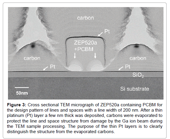
Figure 3: Cross sectional TEM micrograph of ZEP520a containing PCBM for the design pattern of lines and spaces with a line width of 200 nm. After a thin platinum (Pt) layer a few nm thick was deposited, carbons were evaporated to protect the line and space structure from damage by the Ga ion beam during the TEM sample processing. The purpose of the thin Pt layers is to clearly distinguish the structure from the evaporated carbons.
In summary, nanocomposite organic EB resist polymers of ZEP520a containing PCBM are excellent electrically conductive component materials for nanometer lateral-scale electronic devices. Using this material, nanoscale organic electrically conductive structures can easily be fabricated with nanoscale lateral positional control simply by EB exposure and development. The distribution of PCBM aggregations was examined in the nanocomposite organic EB resist polymer. The technique described in this study is applicable to sensitive biosensors having submicron- or nanometer-width channels and Coulomb islands in organic integrated single-chip systems suitable for multiplexed and simultaneous diagnoses. Further investigations on modifying the surfaces of nanocomposite organic EB resist polymers for the purpose of attaching biomaterials are extremely important for biosensors.