Journal of Research and Development
Open Access
ISSN: 2311-3278
ISSN: 2311-3278
Review Article - (2023)Volume 11, Issue 3
The review work on Constant Delay (CD) logic is presented in this paper. Dynamic (Complementary Metal Oxide Semiconductor) CMOS circuit style is introduced, allowing for a reduction in the number of transistors required to implement any logic. (Logical feeding) FTL avoids the use of more transistors in dynamic domino logic by implementing it with the same number of transistors as in dynamic logic. The CD logic generates high-speed operation of potential circuits. The timing window technique is examined, which is primarily used to reduce power dissipation, i.e., to shorten the evaluation time. CD logic has an unusual feature in that the output is pre-evaluated before the input from the previous stage is ready. This property provides a good performance analysis when compared to the dynamic and static logic styles. CD logic reduces charging current with the assistance of leakage current. Different circuits based on CD logic are analyzed for power, delay, (Power Delay Product) PDP, and noise calculation using 90 nm CMOS technology. The CD logic generates high-speed operation of potential circuits. The timing window width technique is examined in order to reduce circuit power consumption while maintaining circuit performance speed. Using 90 nm GPDK CMOS technology, the proposed logic has a much higher average speed than previous works.
Constant delay; CMOS; Logical feeding; Transistors; GDPK
Power dissipation, speed performance, power delay product, and transistor sizing must all be considered in digital design. Several techniques in the low power area have already been proposed by various researchers. The main factor that we require is speed of operations. The fastest growing VLSI technology is increasing on a daily basis. The most commonly used parameters in analyzing circuit performance are average power, delay, noise, and area. Advances in CMOS technology must always priorities improved average power, noise, delay, and area performance. Several dynamic technologies have already been proposed to improve VLSI performance. High performance, energy-efficient circuits have always been prioritized in the field of VLSI circuits. The dynamic CMOS circuit technique is introduced for implementing any logic function with a smaller number of transistors. Various techniques for implementing any logic function, such as dynamic domino logic, pass transistor CMOS logic style, zipper domino, have been proposed, but they have never gained traction in the VLSI field [1-3]. The pull-up network in dynamic logic is swapped by single PMOS transistors driven by the clock, while the pull-down network only consists of NMOS transistors. Use n+2 transistors to implement dynamic logic for an n-bit input. The increased delay drawback of dynamic logic typically occurs during gate cascading. Another disadvantage of dynamic logic is that during the pre-charge phase, regardless of the input applied in the NMOS pull down network, the intermediate node at logic 1 will not be at the output due to current leakage. The other issue is the charge sharing issue. To compensate for the increased delay, domino logic placed an inverter before the output node. Because of switching activity and clock domino logic is not suitable for low power design, but rather for high speed design [4]. Charge redistribution is also a significant disadvantage of this logic, as is the requirement for an additional output inverter.
One solution is the development of dynamic domino logic with a footer transistor, which allows logic designers to implement high-performance circuit operations. Because of the structure of dynamic sdomino logic, it has lower power dissipation and higher speed than static CMOS.
Later, a new methodology called data driven dynamic logic is introduced to remove the nature of non-inversion in domino logic [5]. The input data replaces the clock signal in data driven dynamic logic [6]. This logic style avoids clock routing issues and results in the use of the inverting logic presented [7,8]. When comparing the evaluation path to the propagation path of a cascade network with pre-charging, the propagation path may be slower. To address this issue, a novel logic known as Feedthrough Logic (FTL) is introduced. In FTL, the clock and transistor parts are replaced, and the clock transistor is included in the critical path.
FTL has the disadvantage of higher power dissipation but the advantage of lower noise margin. To deal with this problem, a new logic called Constant Delay (CD) logic was introduced [9].
The remainder of this review work is organized as follows: Section II introduces the CD logic and Feed Through Logic review work (FTL). Section III introduces the need for CD logic and the simulation of CD logic buffer implementation on GPDK-90 nm CMOS process technology. Section IV provides a review of modified CD logic buffer implementation, modified timing block using CD logic, and simulation on the gpdk-90 nm CMOS process technology. Section V provides an overview of LP-HS logic implemented with CD buffers and simulated on gpdk-90 nm CMOS process technology. Section VI is for comparing outcomes. Section VII is the paper's conclusion. Section VII concludes with information on reference papers.
Logic styles
Review of FTL: This section contains PMOS logic blocks as well as NMOS logic blocks. The clock signal controls the transistors PM1 and PM2. When the CLK signal is activated, the pre-discharge period begins, and the output is demolished to ground via PM2. When the CLK signal is low, PM1 turns on, PM2 turns off, and the output is connected to VDD. If the inputs are logic 1, the output enters a mode of contention operation in which transistors in the NMOS pull down network and PM1 conduct current through a low resistance path. If PDN is not turned on, output immediately switches to logic 1 (Figures 1 and 2).
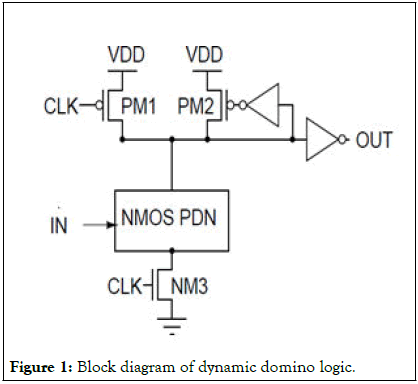
Figure 1: Block diagram of dynamic domino logic.
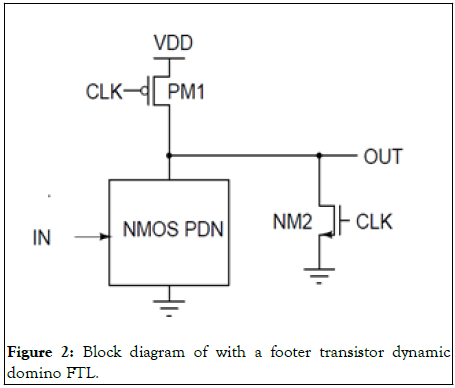
Figure 2: Block diagram of with a footer transistor dynamic domino FTL.
Review of constant delay logic: The designers always need the circuit to respond as quickly as possible, which is why this high clock frequency is required. As we all know, there is a constant demand in the VLSI industry for efficient logic styles that use less energy and operate at a higher frequency. The newly developed Constant Delay logic style (CD) was introduced to overcome large power dissipation, noise at low margins and static power dissipation. It provides a local approximation window technique, which reduces static power dissipation and manages the self-regenerating property of the circuit to enable strong logic operation while consuming less power.
CD logic is introduced to reduce the problems associated with feedthrough logic. It has the unique property of checking the outcome before the input from the previous stage becomes ready.
• Logic block: LB needs to massage the unneeded glitch and
also makes it feasible.
• Timing block: It generates an adjustable window period
to overcome the static power dissipation (Figure 3).
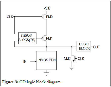
Figure 3: CD logic block diagram.
Buffer implementation using CD logic
Constant delay logic operation: Figure 4 shows a buffer circuit implemented with CD logic. The NOR gate acts as a self-reset circuit, while the series combination of inverters acts as a local window. The primary goal of providing an inverter combination is to produce delay. FTL's support for local window adjustment reduces the contention problem. The NOR gate is a self-resetting circuit with one input from intermediate node X and one applied input that is a delayed clock. The logic block in dynamic domino logic serves as a static inverter. Because we want to stimulate the buffer circuit, we only need one NMOS PDN.
The timing diagram of buffer circuit which we choose to stimulate works with two modes of operation is:
• Evaluation mode (CLK=1)
• Precession mode (CLK=0)
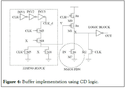
Figure 4: Buffer implementation using CD logic.
When CLK is logic 0, precession mode occurs, and evaluation mode occurs when CLK is logic 1. During the pre-dispose mode, node X and output are both predisposed and precession to GND and VDD. When CLK is high, the CD logic causes nodes X and Y to ground. When CLK is logic 0, three actions occur: Contention, in-out, and CLK-out delay. When IN is high and transistors M1 and CLK are ON, and M2 is off, current flows in a direct low resistance path from PMOS to PDN. X goes to non-zero voltage during this time, and the output waveform has an interim glitch. CLK-out delay occurs when IN is set to 0, indicating that the pull down network is not operational prior to CLK being driven low, and out is discharged, GND, with the delay measured from CLK to out and X rising to logic 1. In-out delay occurs when IN is set to 0 after CLK is set to low; during this phase, X enters contention mode and later switches to logic1, and the delay is measured from in to out. The CD logic timing diagram is shown below (Figure 5).
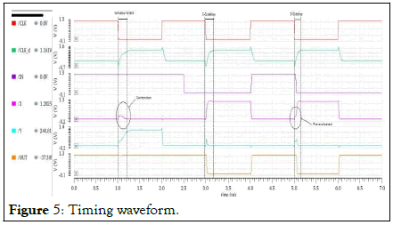
Figure 5: Timing waveform.
A review on modified CD logic and timing block CD logic
Modified CD logic review: The Figure 6 below depicts the CD logic performance on a buffer circuit. The inverter 1 is used to restructure the timing block. The IN and CLK signals are both set to logic high, so M7 and M2 are both turned on, and out is connected to GND. If the pull down network or signal is linked at logic 1, the common node rises to some value and the output end experiences a temporary glitch. When the clock switches from logic 1 to logic 0, the calculation time begins, and three performance phases occur.
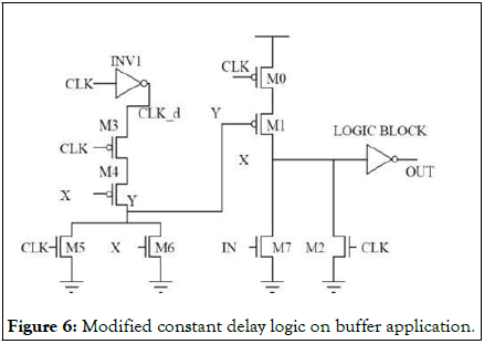
Figure 6: Modified constant delay logic on buffer application.
• If the pull down network is turned on during calculation time,
the common node generates logic 1 and the output end also
generates logic 1. This mode is known as contention mode.
• The IN-out delay mode is used when the applied input
performs a transition when the calculation begins from logic 1
to logic 0 and the output end discharges through VDD.
• The IN-out delay mode is used when the pull down network is
at logic 0 during the calculation period and the out node
discharges to ground.
The inverter size is reduced in order to conserve timing parameters. As a result of the introduction of a new term, transistor sizing, the PMOS transistor should be enlarged. The modified CD logic timing diagram is shown in below Figure 7.
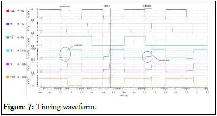
Figure 7: Timing waveform.
CD logic modified timing block: The static power dissipation is reduced by using the timing block to generate an adjustable window period. Logic block must moderate the unnecessary glitch while also making it feasible. The use of transistors for timing blocks is minimized in modified TB constant delay logic style. This decrease in transistors helps to reduce overall power consumption. The overall timing block equation of Y will be Y=(X+CLK) neither using NOR gate. Figures 8 and 9 show the modified TB CD Logic schematic and timing waveform.
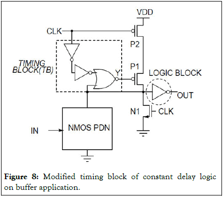
Figure 8: Modified timing block of constant delay logic on buffer application.
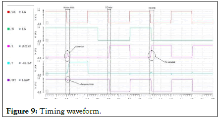
Figure 9: Timing waveform.
Effect of temperature variation on various parameters for conventional circuit
In general, we've compared the power delay product (pdp) in femto joules (fj) to the temperature in degrees celsius. The power delay product (pdp) is an energy measurement that is the product of the average power and the gate delay in the circuit. Figures 10 and 11 depict the sum and carry circuit for the 1-bit full adder pre-layout and post-layout of a conventional Constant Delay (CD) logic circuit that compares the power delay product in fj with the temperature in C. Temperature variations in various circuits are critical for circuit analysis.
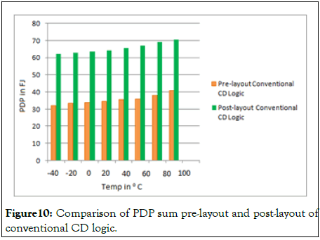
Figure 10: Comparison of PDP sum pre-layout and post-layout of conventional CD logic.
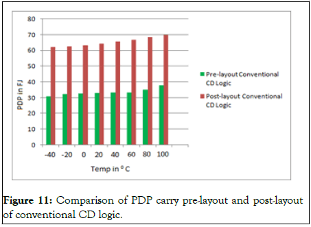
Figure 11: Comparison of PDP carry pre-layout and post-layout of conventional CD logic.
Effect of temperature variation on various parameters for proposed circuit
Figures 12 and 13 depict the sum and carry circuit for the 1-bit full adder, as well as the pre-and post-layout of the modified Constant Delay (CD) logic circuit, which compares the above-mentioned same parameters power delay product in fj with temperature in C. The modified circuit uses bridge style logic, which justifies the change in the carry section of the 1-bit full adder.
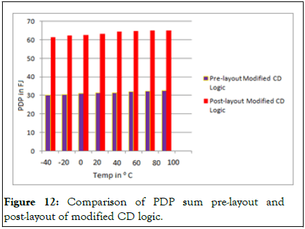
Figure 12: Comparison of PDP sum pre-layout and post-layout of modified CD logic.
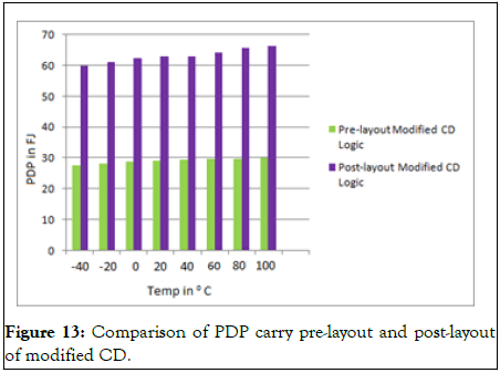
Figure 13: Comparison of PDP carry pre-layout and post-layout of modified CD.
Output noise analysis
Output noise investigation for together pre- layout and post-layout of proposed circuit: The noise in the output is calculated with a 1 MHz offset. The output noise amplitude varies with the input noise amplitude and pulse width. The pulse duration of the output noise varies, and we measure output noise in relation to the variation of the input noise. Calculated output noise for different sum and carry values (Figures 14 and 15).
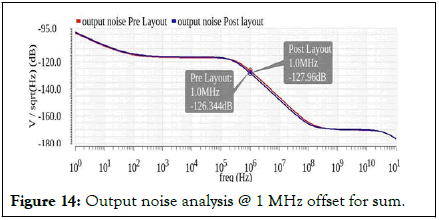
Figure 14: Output noise analysis @ 1 MHz offset for sum.
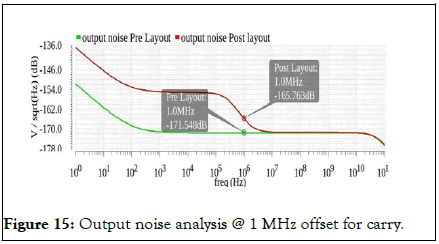
Figure 15: Output noise analysis @ 1 MHz offset for carry.
Comparison
Table 1 and Figure 16 summarize the work we have done in this paper. We have shown average power, noise, delay, and power delay product for C-Q and D-Q parameters for various logic iterations.
| Buffer application (CD logic) | Buffer application (modified CD logic) | Buffer application (modified timing block) | LP-HS (CD logic) | |
|---|---|---|---|---|
| Power (uw) | 28.92 | 17.99 | 4.93 | 18.15 |
| C-Q Delay (ns) | 2.02 | 2.02 | 2.02 | 0.02 |
| D-Q Delay (ns) | 0.52 | 0.52 | 0.52 | 1.48 |
| C-Q PDP (fJ) | 58.5 | 36.41 | 10 | 1.49 |
| D-Q PDP (fJ) | 15.13 | 9.41 | 2.6 | 115.66 |
| Noise (dB) | -157.7 | -157.7 | -162.6 | -172.1 |
Table 1: Data analysis of CD Logic with different parameters.
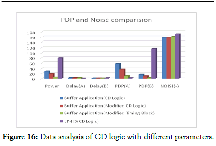
Figure 16: Data analysis of CD logic with different parameters.
In this paper, we analyze four different CD logic based circuits that we simulated on cadence using GPDK 90 nm technology. Power, delay, PDP, and noise are calculated for various CD logic based circuits and compared. It has been discovered that the delay is minimized in all circuits. The speed of operation varies depending on the circuit. The overcome of CD logic from domino logic is enhanced according to the circuit operation requirements. At 1.2 V, simulations for 90 nm complementary MOS technology were run. Every circuit's operational frequency was set to 500 MHz.
Citation: Singh AK, Meher P (2023) Modification of Constant Delay Logic: Design and Analysis. J Res Dev. 11:224.
Received: 18-Jan-2023, Manuscript No. JRD-23-21433; Editor assigned: 20-Jan-2023, Pre QC No. JRD-23-21433 (PQ); Reviewed: 03-Feb-2023, QC No. JRD-23-21433; Revised: 25-Apr-2023, Manuscript No. JRD-23-21433 (R); Published: 02-May-2023 , DOI: 10.35248/2311-3278.23.11.224
Copyright: © 2023 Singh AK, et al. This is an open-access article distributed under the terms of the Creative Commons Attribution License, which permits unrestricted use, distribution, and reproduction in any medium, provided the original author and source are credited.